

Key Takeaways
- TSMC monetizes semiconductor innovation without taking product-design risk. Its core model is the pure-play foundry: customers supply proprietary chip designs, while TSMC sells manufacturing capacity, process technology, yield execution, advanced packaging and related services.
- The strongest moat is switching cost. Moving a leading-edge chip to another foundry is not a simple procurement decision; it can require redesign, EDA and IP requalification, physical implementation changes, packaging rework, reliability validation and a new yield ramp. The economic cost of lost time-to-market can exceed any nominal wafer-price savings.
- TSMC’s second core moat is cost advantage derived from manufacturing scale, yield learning and utilization. Its GIGAFAB model and centralized manufacturing systems spread enormous fixed costs across a broad customer base while accelerating learning across process nodes.
- AI is changing TSMC’s revenue mix, not its corporate DNA. High-performance computing accounted for 66% of second-quarter 2026 revenue, while advanced nodes at 7nm and below represented 77% of wafer revenue. N2, N2P, A16 and advanced packaging therefore matter because they deepen TSMC’s share of the compute stack rather than because TSMC is becoming an AI-chip designer.
- The main risks are capital-intensity, customer concentration, overseas-fab margin dilution, execution risk on new-node ramps, and geopolitical duplication. These risks can reduce returns even if semiconductor demand remains structurally strong.
Taiwan Semiconductor Manufacturing Company, traded in the United States through its NYSE-listed ADS under ticker TSM, was founded in 1987 around a deceptively simple proposition: manufacture semiconductors for other companies without competing against them in end products. That decision created the pure-play foundry model and separated chip design economics from fab ownership. In practical terms, TSMC became neutral manufacturing infrastructure for the semiconductor industry.
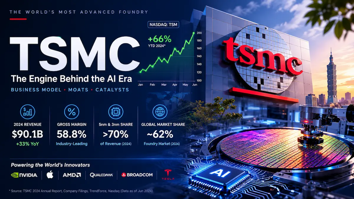
The important point for corporate analysis is that TSMC is no longer merely a factory-for-hire. Its economic architecture now spans leading-edge process technology, manufacturing scale, design enablement, intellectual-property ecosystems, advanced packaging and multi-year capacity planning. The result is a platform that sits underneath smartphones, data-center CPUs, AI accelerators, networking silicon, automotive compute and a growing range of custom chips. As of 2025, TSMC manufactured 12,682 products using 305 technologies for 534 customers, while annual managed capacity exceeded 17 million 12-inch-equivalent wafers.
That platform is currently being pulled toward AI and high-performance computing. In second-quarter 2026, TSMC reported US$40.2 billion of revenue, a 67.7% gross margin and a 60.3% operating margin. HPC represented 66% of quarterly revenue, while 2nm, 3nm, 5nm and 7nm together accounted for 77% of wafer revenue. Through July 2026, reported monthly revenue was up 37.0% year over year on a cumulative basis. These numbers show a business whose growth is increasingly determined by the economics of leading-edge compute, but whose durability still depends on execution rather than demand headlines alone.
1. Business Model Breakdown
TSMC sells manufacturing economics, not branded chips
The TSMC business model is best understood as a capital-intensive technology platform. Customers such as fabless chip designers and integrated device manufacturers bring proprietary designs; TSMC provides the manufacturing process, design rules, production capacity, yield ramp, packaging options and supply assurance needed to turn those designs into commercial silicon. Because TSMC does not market competing branded processors, GPUs or connectivity chips, customers can disclose sensitive roadmaps with less strategic conflict than they would face with a vertically integrated rival.
Wafer fabrication remains the principal revenue engine. According to TSMC’s 2025 Form 20-F, wafer fabrication generated approximately 86% of net revenue. The remaining revenue came mainly from packaging and testing, mask making, design-related services and royalty income. This mix matters because it shows that advanced packaging is strategically important without yet replacing the core economics of wafer manufacturing.
The monetization engine is node mix, utilization, yield and pricing discipline
TSMC does not operate like a commodity manufacturer whose economics are determined only by unit volume. Revenue and profitability are driven by a combination of process-node mix, capacity utilization, yield, customer demand, negotiated pricing and foreign-exchange movements. Advanced nodes generally carry more strategic value because customers are buying more than smaller transistors: they are buying performance per watt, density, time-to-market, production predictability and access to sufficient leading-edge capacity.
This makes yield one of the most economically important variables in the business. Semiconductor fabs have enormous fixed costs. Once equipment is installed, better yield and higher utilization allow more sellable dies to emerge from the same capital base, improving the economics of every wafer. TSMC’s centralized Super Manufacturing Platform is designed to accelerate yield learning, improve production flexibility and shorten time-to-volume across large fabs. That operating system is one reason scale can become an advantage rather than merely a cost burden.
The latest revenue mix illustrates how this mechanism is evolving. In 2025, HPC accounted for 58% of revenue and smartphones 29%. By second-quarter 2026, HPC had risen to 66% while smartphones declined to 22%. At the same time, N2 had already reached 3% of wafer revenue only months after entering high-volume manufacturing in the fourth quarter of 2025. The economic implication is that TSMC is increasingly exposed to customers for whom leading-edge performance, power efficiency and packaging bandwidth are strategic constraints, not discretionary upgrades.
Platform strategy: OIP turns the foundry into an ecosystem
TSMC’s platform strategy is most visible in its Open Innovation Platform, or OIP. Launched in 2008, OIP links process technology with electronic design automation, silicon-proven IP, design services, cloud infrastructure and advanced packaging. The commercial objective is to reduce design barriers and shorten the path from chip architecture to working silicon.
This matters because semiconductor manufacturing cannot be separated cleanly from design. A customer choosing a leading-edge node also needs validated design rules, libraries, interface IP, verification flows, timing models and packaging methodologies. OIP therefore extends TSMC’s role upstream into design enablement without requiring the company to own the customer’s product architecture. That is a strategically elegant model: TSMC captures more ecosystem influence while preserving the neutrality that made the foundry model valuable in the first place.
Advanced packaging is the next layer of that platform. TSMC’s 3DFabric portfolio includes CoWoS, InFO and SoIC technologies that integrate logic, chiplets and high-bandwidth memory. CoWoS has been in volume production since 2012, but generative AI materially increased demand because large accelerators require enormous memory bandwidth and increasingly complex multi-die integration. In this environment, packaging is no longer a low-value backend step; it can determine system performance, power efficiency, memory bandwidth and achievable compute density.
The business model is therefore becoming more vertically complete without becoming vertically competitive. TSMC still does not need to design the accelerator, CPU or smartphone SoC. Instead, it monetizes more of the manufacturing and integration stack that those products require.
2. Deep Dive into Economic Moats
Primary moat: Switching Costs
The most defensible component of TSMC’s economic moat is switching cost. This is not contractual lock-in in the conventional software sense. It is engineering lock-in created by the interaction of process technology, design tools, IP, manufacturing learning and product qualification.
A leading-edge chip is physically designed around a foundry’s process design kit, transistor architecture, standard-cell libraries, memory macros, timing characteristics, power-delivery assumptions and manufacturing rules. Porting that product to a competing foundry can require substantial redesign, new physical verification, different IP, fresh tape-outs, reliability qualification and a new yield ramp. For advanced AI and HPC products, packaging architecture may also need to be reworked because logic, HBM, interposers and thermal constraints are co-optimized as a system.
The switching cost is therefore measured less by engineering fees than by schedule risk. A delayed accelerator generation can miss a hyperscaler deployment cycle; a delayed smartphone SoC can miss a device launch; a failed tape-out can destroy months of product economics. TSMC management has emphasized that technology selection, product development, capacity preparation and high-volume ramp can take more than five years. That duration is itself a moat because a competitor cannot erase customer qualification history with a single capital-spending announcement.
What would a rival need to spend to overcome this moat? Not only tens of billions of dollars on fabs and equipment, but also years building process maturity, EDA certification, reusable IP, packaging capability, customer engineering relationships and a credible record of high-volume yield. The capital is necessary, but it is not sufficient.
Primary moat: Cost Advantages
TSMC’s second core moat is structural cost advantage, although it should be described carefully. The advantage is not simply that TSMC is large. Scale becomes a moat only when it lowers unit cost, improves utilization, accelerates learning or increases purchasing and operating efficiency.
TSMC’s GIGAFAB model does exactly that. Large, centrally managed fabs allow the company to spread fixed costs across greater output, move learning more quickly through the manufacturing network, support demand fluctuations and reduce the cost of product requalification. A broad customer base also improves the probability that capacity can be redeployed across applications and process families rather than sitting idle when a single end market slows.
Yield learning compounds this advantage. Higher production volume generates more process data, which can improve defect detection, equipment matching and process control. Better yield then lowers effective cost per good die and can support stronger margins or more competitive pricing. This creates a flywheel between scale and manufacturing knowledge that is difficult for a smaller competitor to reproduce because the learning is embedded in operations, not purchased off the shelf.
However, the cost moat is not invulnerable. TSMC’s global expansion is deliberately adding redundancy and geographic proximity, but overseas fabs are more expensive. In July 2026, management said overseas-fab ramp-up could dilute gross margin by roughly 2 to 3 percentage points in early stages and 3 to 4 points in later stages. The moat therefore survives only if TSMC can preserve enough technology differentiation, pricing power and utilization to offset the structural cost of geographic duplication.
Intangible Assets: Important, but embedded rather than standalone
TSMC also benefits from intangible assets, particularly process know-how, customer trust and accumulated manufacturing data. These assets matter because semiconductor customers expose long-range product roadmaps and rely on the foundry to protect intellectual property, reserve capacity and execute on schedule. Trust lowers friction in those relationships.
Still, it would be analytically weak to label “brand” as the primary moat. TSMC’s reputation has economic value because it is backed by process results, yield, confidentiality and delivery performance. If those operating fundamentals deteriorated, brand recognition alone would not protect the franchise.
Network Effects: A reinforcing ecosystem effect, not a classic consumer network
OIP creates a real but indirect network effect. As more customers design on TSMC processes, EDA vendors, IP suppliers, cloud providers and design-service partners have stronger incentives to certify and optimize their tools for those nodes. Better ecosystem readiness lowers customer design friction, which can attract more design activity back to TSMC.
That loop reinforces switching costs, but it should not be confused with a social-network effect where every new user directly increases the product’s utility to every other user. Semiconductor customers do not benefit simply because another chip company uses the same foundry. They benefit because partner investment in tools, IP and validated flows makes the platform easier and safer to use. The network effect is therefore complementary rather than the principal moat.
From a Buffett-style perspective, the long-term excess-return case rests primarily on switching costs plus cost advantages. Those defenses can support superior economics as long as TSMC stays near the technology frontier and does not overbuild capacity. If process leadership weakens, customer qualification costs become less protective; if utilization falls sharply, manufacturing scale can turn from advantage into fixed-cost burden.
3. Business Inflection Points & Future Catalysts
The strategic inflection point: OIP transformed TSMC from a foundry into industry infrastructure
TSMC’s founding in 1987 established its core gene: pure-play neutrality. The more important strategic inflection after that foundation came in 2008, when the company launched the Open Innovation Platform. That move institutionalized the idea that a foundry could own more of the innovation interface without competing in customer products.
Before OIP, the economic relationship could be viewed primarily as design-to-fab. After OIP, the relationship became ecosystem-to-silicon. EDA vendors, IP suppliers, design houses and later cloud and advanced-packaging partners became coordinated around TSMC process readiness. This expanded the competitive battlefield from transistor performance to total design enablement and time-to-revenue.
That distinction is critical today. At leading nodes, the product is no longer just a wafer process. The product is an integrated development environment that includes manufacturing, design tools, reusable IP, packaging and the confidence that capacity will be available when the customer needs to ramp. OIP made that platform logic explicit years before chiplet architectures and AI packaging made system integration a headline issue.
Catalyst 1: N2, N2P and A16 can extend leading-edge revenue mix
The first 12-to-24-month catalyst is the ramp of the N2 family. N2 entered high-volume production in the fourth quarter of 2025 and contributed 3% of wafer revenue in second-quarter 2026. N2P and A16 are scheduled for volume production in the second half of 2026. A16 combines nanosheet transistors with TSMC’s Super Power Rail backside power-delivery architecture and is targeted at HPC designs with dense routing and demanding power networks.
The transmission mechanism is straightforward: if customers adopt these nodes for flagship AI accelerators, CPUs, custom ASICs and premium mobile processors, a larger share of TSMC’s wafer mix migrates toward leading-edge technologies. That can support revenue growth because advanced-node demand is tied to increasing compute intensity and because customers are purchasing scarce manufacturing capability with high strategic value.
The observable indicators are N2’s quarterly share of wafer revenue, the percentage of revenue from 7nm-and-below technologies, HPC platform growth, and whether N2P/A16 enter volume production on schedule. Gross-margin behavior also matters. Management expects the steep N2 ramp to dilute gross margin by roughly 3 to 4 percentage points in the second half of 2026 before learning-curve improvements and utilization can offset part of the drag.
The principal execution risks are yield maturation, customer product delays and an unfavorable mix between new-node startup costs and mature-node profitability. A technically successful node can still be economically disappointing if ramp costs arrive before customer volume or if competing process alternatives become credible enough to force pricing concessions.
Catalyst 2: Advanced packaging can increase TSMC’s share of AI system value
The second catalyst is the scaling of CoWoS, SoIC and the broader 3DFabric portfolio. AI accelerators increasingly require logic to be integrated with multiple HBM stacks and chiplets. That pushes value from a single monolithic die toward a system-level package, exactly where TSMC has been building capability for more than a decade.
The transmission mechanism is not merely additional packaging revenue. Advanced packaging can make TSMC’s front-end process more attractive because customers prefer a validated path from logic die to full heterogeneous integration. The more tightly process technology and packaging are co-designed, the more difficult it becomes to treat foundry selection as a standalone wafer-price decision.
Observable indicators include TSMC’s advanced-packaging capital allocation, the mix of HPC revenue, evidence of continued CoWoS capacity expansion, and customer adoption of larger multi-die architectures. TSMC said roughly 10% to 20% of its 2026 capital budget would go to advanced packaging, testing, mask making and other areas, providing a direct signal that backend integration is becoming a larger capital priority.
Risks include bottlenecks outside TSMC’s direct control, such as HBM supply, substrates, testing capacity and customer system deployment schedules. In addition, hyperscalers and chip designers may diversify packaging suppliers where technically feasible. The moat therefore depends on integration quality and time-to-market, not simply capacity scarcity.
Catalyst 3: Geographic capacity can deepen customer commitments, but it is a margin trade-off
The third catalyst is geographic expansion. TSMC’s Arizona investment has expanded to US$265 billion, and the company said in July 2026 that it intends to build several additional 2nm-and-below logic fabs as well as advanced-packaging facilities to support strong U.S. customer demand. In parallel, TSMC continues to add advanced capacity in Taiwan and expand in Japan and Europe.
The transmission mechanism is strategic assurance. Large U.S. customers increasingly value geographic resilience, supply-chain redundancy and local access to advanced manufacturing. If customers are willing to make longer-range capacity commitments in return for that resilience, overseas fabs can reinforce the switching-cost moat and reduce the perceived risk of concentrating all leading-edge production in one geography.
The observable indicators are fab construction milestones, start-of-production dates, customer volume commitments and the margin performance of overseas operations. TSMC’s rising 2026 capital budget of US$60 billion to US$64 billion is also a useful signal; management said roughly 70% to 80% would be allocated to advanced process technologies.
The risk is that resilience is expensive. Labor, construction, supplier density and operating costs outside Taiwan can be less favorable. If customers do not pay enough for geographic diversification, overseas capacity can raise revenue while reducing returns on invested capital. Policy changes, project delays and duplicative global capacity are additional risks.
Near-term operating context: strong demand does not eliminate cycle risk
TSMC’s current operating momentum is unusually strong. Management guided third-quarter 2026 revenue to US$44.6 billion to US$45.8 billion and said full-year U.S.-dollar revenue growth should be slightly above 40%. July 2026 monthly revenue rose 44.7% year over year. These figures confirm that AI demand is already converting into reported revenue rather than remaining a distant forecast.
But the semiconductor cycle still matters. Consumer and price-sensitive end markets can weaken even while AI remains robust. Customer concentration also deserves attention: in 2025, TSMC’s ten largest customers accounted for approximately 78% of net revenue, while the two largest represented 19% and 17%, respectively. A business can have a powerful moat and still experience earnings volatility if a few customers change product cadence or inventory strategy.
4. Key FAQs
How does TSMC make money and what drives its gross margin?
TSMC primarily makes money by manufacturing customer-designed semiconductors. Wafer fabrication accounted for about 86% of 2025 net revenue, with the rest mainly coming from packaging and testing, mask making, design-related services and royalties. Gross margin is driven by process mix, wafer pricing, capacity utilization, yield, cost improvement, new-node startup costs, overseas-fab economics and foreign exchange. In practical terms, a mature high-yield fab running near efficient utilization is more profitable than a newly ramping node, even if the new node has greater strategic value.
Why is the TSMC business model hard for Intel or Samsung to replicate?
The difficult part is not building a fab; it is reproducing the full system around the fab. A credible competitor needs process technology, high-volume yield, enough capacity to absorb large product ramps, EDA and IP readiness, advanced packaging, confidentiality, long customer qualification histories and the willingness to support customers whose products may compete with the foundry owner’s internal businesses. TSMC’s pure-play structure removes one strategic conflict by design, while decades of ecosystem integration increase the engineering cost of switching.
How does TSMC benefit from AI if it does not design AI chips?
TSMC benefits from AI by supplying the manufacturing bottlenecks that advanced compute requires. AI accelerators, custom ASICs, data-center CPUs and networking silicon demand leading-edge logic, high transistor density, power efficiency and sophisticated integration with HBM. TSMC monetizes those requirements through advanced wafers and 3DFabric packaging. The company therefore has broad exposure to AI compute spending across multiple chip architectures without having to predict which individual accelerator brand or instruction set ultimately wins.
5. Conclusion
TSMC’s corporate gene is neutrality converted into infrastructure. The company began by separating chip design from fab ownership, then compounded that advantage by building the manufacturing scale, process know-how and customer trust required to make outsourcing strategically safe. OIP extended that model into design enablement, while 3DFabric is extending it again into system-level integration.
The company’s strongest economic defenses are switching costs and cost advantages. Customers become embedded in TSMC’s process, IP, EDA and packaging ecosystem, while TSMC’s scale and yield-learning system lower the effective cost and risk of bringing complex chips to volume. Network effects and intangible assets reinforce those defenses, but they are not substitutes for manufacturing execution.
Over the next one to two years, the central question is not whether AI demand exists; current revenue already demonstrates that it does. The more important question is whether TSMC can convert the N2/N2P/A16 cycle, advanced-packaging expansion and global capacity build-out into profitable growth without allowing new-node startup costs and overseas duplication to erode returns. The enterprise remains structurally advantaged, but the durability of that advantage will continue to be earned through yield, capital discipline and customer trust rather than market position alone.
Official Sources and External Links
- TSMC Company Profile
- TSMC 2Q26 Quarterly Results
- TSMC 2026 Monthly Revenue
- TSMC 2025 Form 20-F — U.S. Securities and Exchange Commission
- TSMC 2025 Annual Report Website
- TSMC Debuts A13 Technology at 2026 North America Technology Symposium
- TSMC HPC Platform — Advanced Technologies
- TSMC Open Innovation Platform
- TSMC: Celebrating 15 Years of OIP Ecosystem Collaboration
- TSMC CoWoS Advanced Packaging
- TSMC GIGAFAB Facilities
- TSMC Arizona
Disclaimer: This article is intended solely for business logic discussion and corporate research purposes, and does not constitute investment advice of any kind.